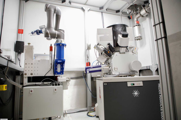
The Focussed Ion Beam (FIB) can be used for high-resolution imaging (as in a SEM) and as a tool to machine micron-scale test pieces into the surface of a sample. It does this by bombardment with high-energy gallium ions, removing material via sputtering in a pattern defined by the user.
Overview
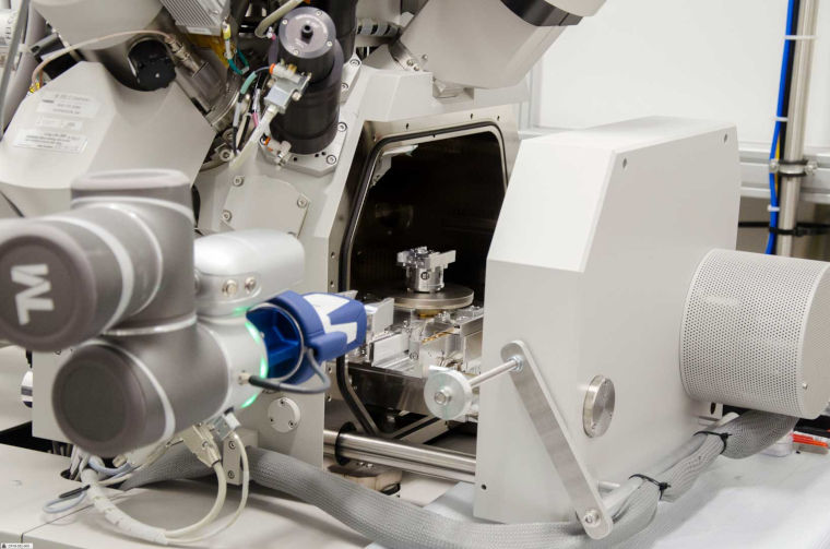
Owing to small spot size associated with the conventional gallium ion source, this instrument is well-suited to high precision micromachining applications such as the preparation of TEM lamella or APT needles, where the final sample is on the order of ~100 nm in thickness / diameter. The FIB is also equipped with Pt, C and W gas injection systems (GIS) for deposition of protective layers, and a Nanomanipulator needle for lift-out or manipulation of test pieces,
A range of electron and secondary ion detectors allow for high resolution imaging. Complimentary analytics in the form of an EBSD camera allows for the acquisition of crystallographic information (phase distribution, crystallographic orientation, grain size and morphology), which facilitates targeted specimen preparation and lift out according to phase distribution or crystallographic orientation. High resolution crystallographic orientation information can also be obtained from electron transparent samples using Transmission Kikuchi Diffraction.
FEI’s AutoTEM™ software packages allow automated TEM lamella preparation. Auto Slice and View™ enables small-scale 3D tomography, which can be used in conjunction with the EBSD camera to obtain 3D volumetric information including EBSD data where required.
Optional use of the Cryo Stage enables micromachining / ion milling of samples at cryogenic temperatures. This instrument is also equipped with a Vacuum Cryo Transfer system which enables transfer of test pieces to and from compatible experimental apparatus under vacuum and cryogenic conditions (See also: Leica VCT 500 Cryo Stage and Vacuum Cryo Transfer System).
Applications
- TEM lamella preparation
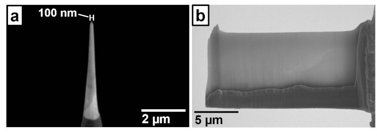
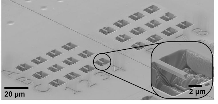
- Atom Probe Tomography (APT) needle preparation
- Microcantilever preparation
- Surface or cross-sectional EBSD analysis (phase distribution, crystallographic orientation, grain size and morphology)
- Small-scale 3D tomography and / or 3D EBSD analysis
- High-resolution Imaging
- Transmission Kikuchi Diffraction analysis (ultra-high-resolution phase distribution, crystallographic orientation, grain size and morphology)
- Micromachining and/or sample preparation (e.g. TEM / APT) at cryogenic temperatures
Technical specification
- Schottky thermal field-emission electron gun for high-resolution imaging
- Gallium ion source for milling
- Pt, C and W deposition capabilities
- Large voltage and probe current range:
- Electron-beam: 200 V – 30 Kv, 0.7 pA – 22 nA
0.9 nm resolution (15 kV) - Ion-beam: 500 V – 30 kV, 0.1 pA – 65 nA
4.5 nm resolution (30 kV)
- Electron-beam: 200 V – 30 Kv, 0.7 pA – 22 nA
- 5-axes stage with -10 – +60° tilt range, infinite rotation
- Chamber and in-lens electron detectors, dedicated retractable BSE detector
- Oxford Instruments Symmetry S2 EBSD camera (>4500 EBSP / s, 0.05° angular resolution)
- Optional Cryo stage (<-140°C – +20°C Temperature range, ±1°C temperature regulation)
Materials Research Facility
Available for users working in fusion, fission and other research programmes. We have scientific and operational teams to support experiments and sample preparation.